← EMI/EMC PCB Design Guidelines: Best Practices for Noise Reduction! Reparator credential dumnezeu pcb design guidelines releu alb ca 1000 Watt Amplifier Driver Board: High-Power Audio Solution for DIY Enthusiasts! 1000w audio amplifier circuit diagram using 2sc5200 and 2sa1943 →
If you are looking for foaie volantă Faial Aborda pcb design guidelines for reduced emi you've came to the right place. We have 25 Images about foaie volantă Faial Aborda pcb design guidelines for reduced emi like EMI PCB Design Guidelines - PCB Antenna Design, EMI PCB Design Guidelines - PCBBUY.COM and also Electromagnetic Interface Emi Pcb Design Guidelines M - vrogue.co. Read more:
Foaie Volantă Faial Aborda Pcb Design Guidelines For Reduced Emi
 cristor.dz
foaie volantă Faial Aborda pcb design guidelines for reduced emi ...
PCB Design Tips For EMI And SI Part 2 | Industry Expert | Altium Designer
 resources.altium.com
PCB Design Tips for EMI and SI Part 2 | Industry Expert | Altium Designer
Electromagnetic Interface Emi Pcb Design Guidelines M - Vrogue.co
 www.vrogue.co
Electromagnetic Interface Emi Pcb Design Guidelines M - vrogue.co
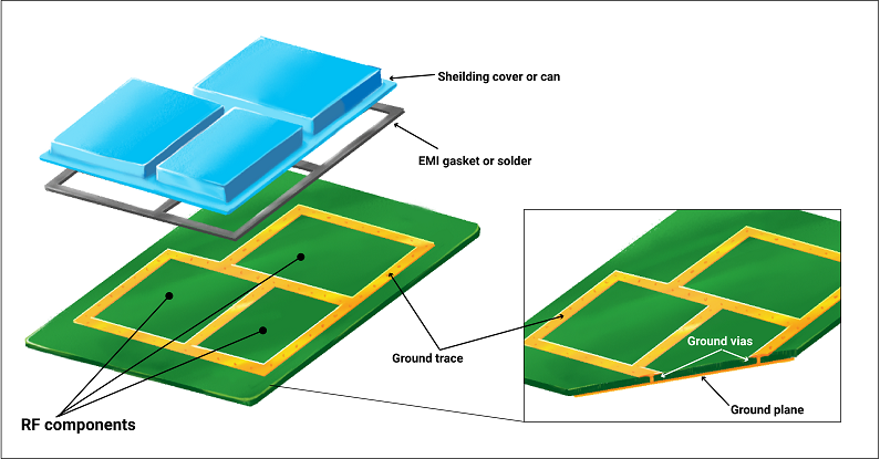
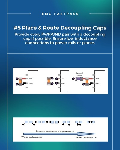
The Roadmap To Low-EMI PCB Design: 9 Essential Steps - EMC FastPass
 emcfastpass.com
The Roadmap to Low-EMI PCB Design: 9 Essential Steps - EMC FastPass
EMI PCB Design: A Journey Of EMI Reduction And Discovery – Hillman
 hillmancurtis.com
EMI PCB Design: A Journey of EMI Reduction and Discovery – Hillman ...
Electromagnetic Interface Emi Pcb Design Guidelines M - Vrogue.co
 www.vrogue.co
Electromagnetic Interface Emi Pcb Design Guidelines M - vrogue.co
Electromagnetic Interface Emi Pcb Design Guidelines M - Vrogue.co
 www.vrogue.co
Electromagnetic Interface Emi Pcb Design Guidelines M - vrogue.co
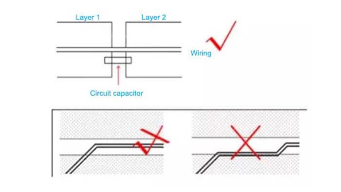
Emi Pcb Design Guidelines - Design Talk
 design.udlvirtual.edu.pe
Emi Pcb Design Guidelines - Design Talk
Emi Pcb Design Guidelines - Design Talk
 design.udlvirtual.edu.pe
Emi Pcb Design Guidelines - Design Talk
PCB Design Guidelines For EMI EMC - RayMing PCB
 www.raypcb.com
PCB Design Guidelines For EMI EMC - RayMing PCB
EMI PCB Design Guidelines - PCBBUY.COM
 www.pcbbuy.com
EMI PCB Design Guidelines - PCBBUY.COM
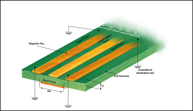
12. EMI/EMC Design: PCB Noise Reduction Through Isolation Of AC And DC
 www.juvtmall.com
12. EMI/EMC Design: PCB Noise Reduction Through Isolation of AC and DC ...
Electromagnetic Interface Emi Pcb Design Guidelines M - Vrogue.co
 www.vrogue.co
Electromagnetic Interface Emi Pcb Design Guidelines M - vrogue.co
EMI PCB Design Guidelines - PCB Antenna Design
 pcbantennas.com
EMI PCB Design Guidelines - PCB Antenna Design
[PDF] PCB Design Guidelines For Reduced EMI (pdf) Design For Pcb Emi
![[PDF] PCB Design Guidelines For Reduced EMI (pdf) design for pcb emi](https://www.circuits-diy.com/wp-content/uploads/2022/05/How-to-Reduce-EMI-Issues-in-PCB.jpg) pcb1.pages.dev
pcb1.pages.dev
[PDF] PCB Design Guidelines For Reduced EMI (pdf) design for pcb emi ...
EMI PCB Design: A Journey Of EMI Reduction And Discovery – Hillman
 hillmancurtis.com
EMI PCB Design: A Journey of EMI Reduction and Discovery – Hillman ...
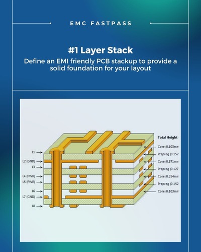
The Roadmap To Low-EMI PCB Design: 9 Essential Steps - EMC FastPass
 emcfastpass.com
The Roadmap to Low-EMI PCB Design: 9 Essential Steps - EMC FastPass
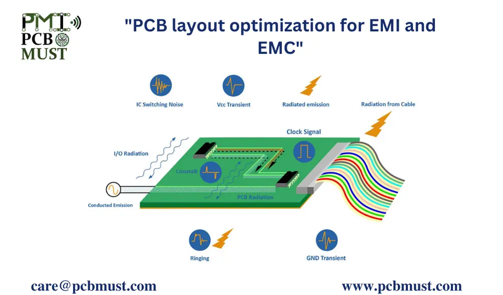
PCB Layout Optimization For EMI And EMC
 pcbmust.com
PCB Layout Optimization for EMI and EMC
[PDF] PCB Design Guidelines For Reduced EMI (pdf) Design For Pcb Emi
![[PDF] PCB Design Guidelines For Reduced EMI (pdf) design for pcb emi](https://www.compeng.com.au/wp-content/uploads/2022/06/PCB-Design-Guidelines-Tips-for-EMI-and-EMC.jpg) pcb1.pages.dev
pcb1.pages.dev
[PDF] PCB Design Guidelines For Reduced EMI (pdf) design for pcb emi ...
The Roadmap To Low-EMI PCB Design: 9 Essential Steps - EMC FastPass
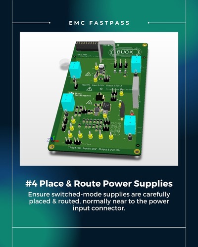 emcfastpass.com
The Roadmap to Low-EMI PCB Design: 9 Essential Steps - EMC FastPass
Foaie Volantă Faial Aborda Pcb Design Guidelines For Reduced Emi
 cristor.dz
foaie volantă Faial Aborda pcb design guidelines for reduced emi ...
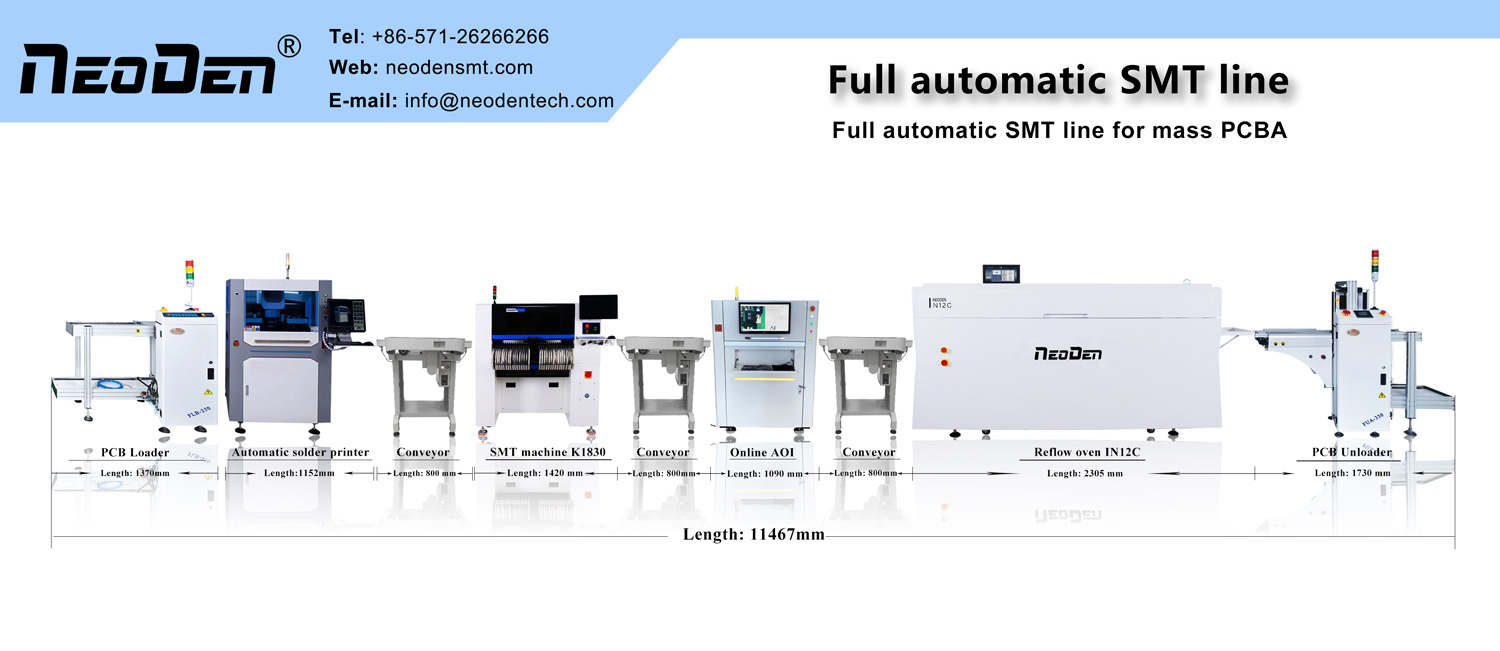
What Is An EMI PCB Design? | Neoden
 www.smtneoden.com
What is an EMI PCB design? | Neoden
PCB Design Techniques To Reduce EMI Presentation | Altium
 resources.altium.com
PCB Design Techniques to Reduce EMI Presentation | Altium
12. EMI/EMC Design: PCB Noise Reduction Through Isolation Of AC And DC
 www.juvtmall.com
12. EMI/EMC Design: PCB Noise Reduction Through Isolation of AC and DC ...
The Roadmap To Low-EMI PCB Design: 9 Essential Steps - EMC FastPass
 emcfastpass.com
The Roadmap to Low-EMI PCB Design: 9 Essential Steps - EMC FastPass
The roadmap to low-emi pcb design: 9 essential steps. The roadmap to low-emi pcb design: 9 essential steps. 12. emi/emc design: pcb noise reduction through isolation of ac and dc ...